SE050 Breakout
NXP EdgeLock SE050E2HQ1 secure element on a 5-pin 2 mm header
16.42 × 14.56 mm · two layers · I²C at 0x48
1. Overview
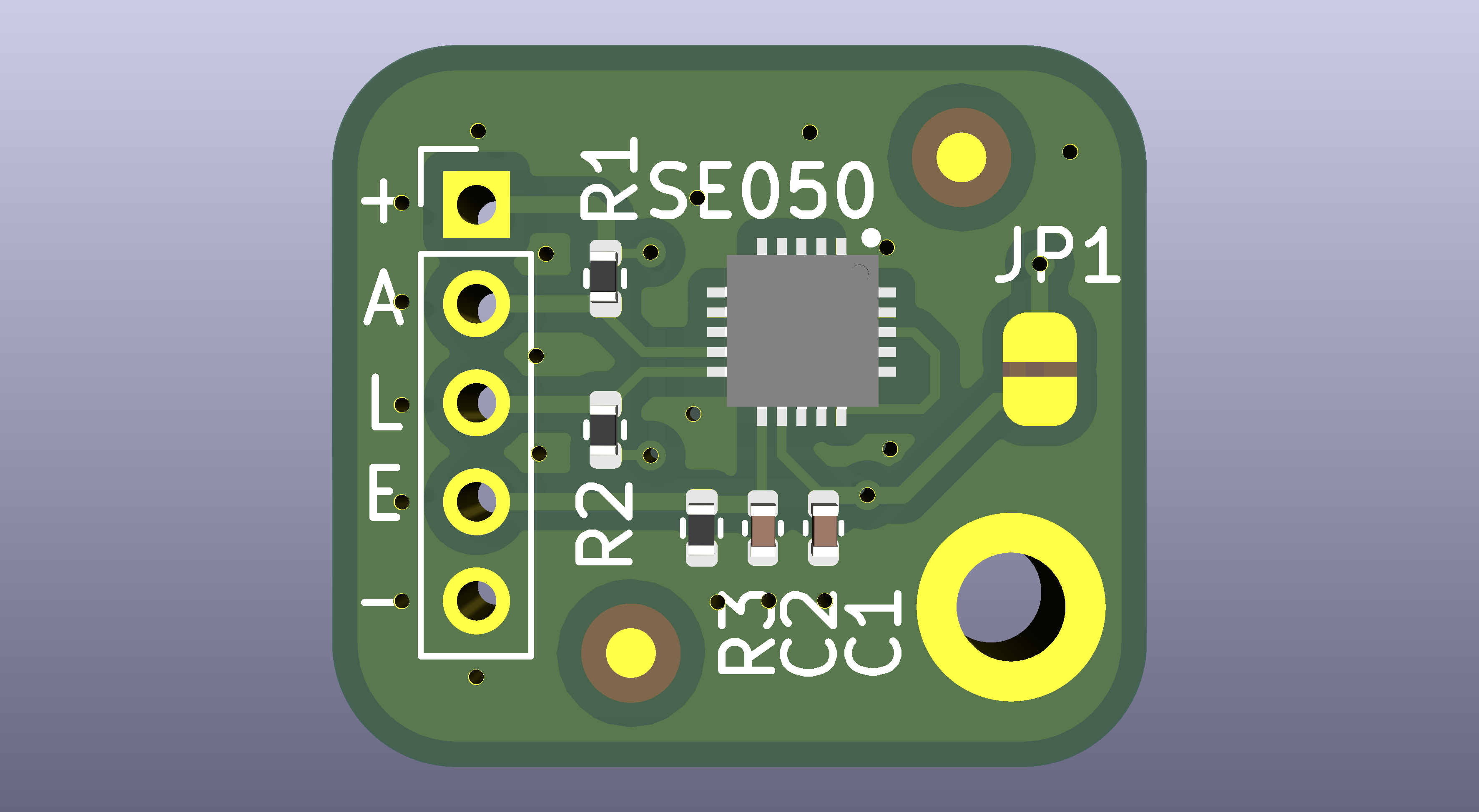
A minimal breakout board for the NXP EdgeLock SE050E2HQ1 secure element, bringing the I²C interface out to a 5-pin 2 mm header. 16.42 × 14.56 mm, two layers, all passives 0402.
Key features
- NXP EdgeLock SE050E2HQ1 — a Common Criteria EAL 6+ secure element for key storage, ECC and AES operations, and secure provisioning
- I²C target at address 0x48, with 4.7 kΩ pull-ups already on the board
- ENA broken out to the header, so the host gets a hard power switch over the chip — deep power-down draws under 5 µA
- JP1 solder jumper ties ENA high permanently, for hosts with no pin to spare
- Designed in KiCad 10 and self-contained: symbol, footprint and 3D model live in the repository, so it opens anywhere without installing extra libraries
- Two fiducials and a machine-ready gerber set, for automated assembly
2. Pinout
J1 — 1×5, 2 mm pitch
| Pin | Net | Notes |
|---|---|---|
| 1 | +3.3V | Supply, feeds VIN (pin 12) |
| 2 | SDA | I²C data, 4.7 kΩ pull-up on board |
| 3 | SCL | I²C clock, 4.7 kΩ pull-up on board |
| 4 | ENA | Enable — drive high to use the chip, or close JP1 |
| 5 | GND |
ENA is not optional — this is the first thing to get wrong
R3 pulls ENA to ground, so the SE050 powers up in deep power-down and will not answer on I²C until ENA goes high. If your scan of the bus finds nothing at 0x48, this is almost certainly why.
- Drive ENA from a GPIO (pin 4 of the header). This is the reason the pin is broken out: it gives the host a hard power switch over the secure element, and deep power-down draws under 5 µA.
- Close JP1 if you have no pin to spare. It is a solder jumper on the top side, labelled on the silkscreen, and it ships open — bridge the two pads and the chip is permanently enabled. Leave pin 4 unconnected in that case.
Closing JP1 costs you only the deep power-down mode. Software power-down (~430–480 µA, with state retention, woken by a falling edge on SDA) still works either way. It also leaves R3 as a permanent 100 kΩ load across the rail, about 33 µA.
3. Bill of Materials
| Ref | Value | Footprint | LCSC | Purpose |
|---|---|---|---|---|
| SE050 | SE050E2HQ1/Z01Z3Z | HX2QFN20 3×3 mm | C5190917 | Secure element |
| C1 | 100 nF | 0402 | C1525 | VIN decoupling |
| C2 | 33 nF | 0402 | C106862 | ENA filtering |
| R1, R2 | 4.7 kΩ | 0402 | C105871 | I²C pull-ups to 3V3 |
| R3 | 100 kΩ | 0402 | C60491 | ENA pull-down |
| J1 | 1×5 header | 2 mm pitch | — | Breakout header |
| JP1 | — | Solder jumper, top side | — | Ties ENA to 3V3; ships open |
| H1 | — | M2 | — | Mounting hole, tied to GND |
| FID1, FID2 | — | 1 mm fiducial | — | Optical alignment for automated assembly |
Only the five parts with an LCSC number are fitted by machine; J1, JP1 and H1 are hand work or nothing at all.
4. Design Notes
Worth reading before you reuse this in your own layout — most of it comes straight from the SE050 data sheet and is easy to get wrong.
No capacitor between VOUT and VCC
Application note AN13483 §8.2.2 asks for that node to be left undecoupled on an I²C part that uses deep power-down, and this board follows it. Two builds were made to test the point — one with a 33 nF there and one without — and they were indistinguishable across every measurement available without an oscilloscope: identical enable/disable timing, identical 1 µA deep power-down current, and the same result on every functional test. The note is obeyed because obeying it costs nothing, not because a failure was reproduced.
The ISO7816 pins are left unconnected on purpose
The SE050 also speaks ISO7816 and ISO14443 as a smart card, but that interface is not enabled in generic SE050 configurations — NXP enables it only on customer request (see AN12436, which does not list it for any stock part number). On the E2 those pads are inert, and the data sheet's own recommendation for pins 3 (IO1), 13 (CLK) and 16 (IO2) is “n.c. (recommended)”.
Pin 14 (RST_N) is the exception, and it goes to ground
For that pad the data sheet offers no floating option — “if not used then connect to VCC or VSS” — and of the two, VSS is the one that holds up in every state of this board. RST_N is referenced to VCC, and VCC is fed from VOUT through an internal switch that opens in deep power-down: with ENA low, VCC drops to 0 V while VIN stays up, so a pin tied to the 3V3 rail would sit above its own reference. Ground sidesteps that, and it cannot hold the part in reset because RST_N is only active when the ISO7816 interface is enabled, which it is not on the E2.
Note that IO1 and IO2 double as the I²C controller pins (SDA and SCL respectively) — the SE050 acting as a bus master to talk directly to a sensor and sign its readings. The E2 supports that at up to 1 Mbit/s. If you want it, those are the pads to break out.
VOUT is a switch, not a regulator
Pin 15 (VOUT) supplies pin 18 (VCC) through an internal power switch of about 1.1 Ω, which is why they are tied together here — the arrangement the data sheet requires for deep power-down to work. In deep power-down VOUT and VCC are switched off entirely and only the I²C pads stay supplied from VIN.
The exposed pad is ground
It is stitched to the ground plane with five 0.6 mm vias (0.3 mm drill) — four at the corners and one in the centre — leaving 0.175 mm of clearance at the tightest to the edge of the 1.95 × 1.95 mm pad. If you have the stencil made, check that your fab tents the via barrels, or solder will wick down them during reflow.
Two fiducials, diagonally opposite
Each is a 1 mm copper dot in a 2 mm solder mask opening, with a 3 mm keepout drawn as a rule area on the top copper so the ground pour backs away and leaves the camera a clean target. If you hand-solder this board they are simply two bare copper dots and you can ignore them. The keepout is a top-layer rule: the bottom pour runs straight under the fiducials, which is fine, because the camera cannot see through the board.
5. Fabrication
Everything the board house needs is in gerber/, unzipped:
- Gerbers for both copper layers, both solder masks, the top silkscreen and the board outline
- Paste layers for both sides (.gtp / .gbp), for ordering a stencil
- Excellon drill files, plated and non-plated separately, plus drill maps
There is no bottom silkscreen — the layer is empty and is not exported, which keeps the board on the cheaper single-sided legend option. Two-layer board, 1.6 mm, no controlled impedance, nothing exotic. Copper pours are filled in the exported gerbers.
Fabrication status, precisely
An earlier revision of this layout — same schematic, same stack-up, 16.33 × 12.72 mm and without the fiducials — was manufactured, assembled by hand and validated on hardware: the SE050 answers on 0x48, a full SCP03 session opens, keys are generated and survive a power cycle, deep power-down measures 1 µA, and 30 consecutive enable/disable cycles ran without a fault. The solder jumper JP1 was exercised too.
The revision in this repository has not itself been fabricated. It differs by the two fiducials, their keepouts and a slightly larger outline; nothing in the circuit changed. Treat a first order as a prototype run and check it before committing to a batch.
6. GitHub Repository
The complete KiCad 10 project, gerbers, bill of materials and documentation are published under GPL-3.0. The project is self-contained: the SE050 symbol, footprint and 3D model live in the repository, so it opens on any machine without installing extra libraries.
7. Using It with Meshtastic
The board is a plain I²C peripheral at 0x48, so it drops onto any Meshtastic node with a free I²C bus and a 3.3 V rail.
One thing to know before you wire it up: firmware commonly ignores the ENA pin — the Meshtastic SE050 driver, for one, never touches it. If you are dropping this board under existing software, close JP1 and leave pin 4 of the header unconnected. Otherwise the chip stays in deep power-down and the bus scan comes back empty.
If your firmware does drive ENA, wire pin 4 to a spare GPIO instead and leave JP1 open. That buys you the deep power-down mode and a hard power switch over the secure element.
8. Get One Assembled
Want one ready to go? We sell the fully assembled and tested board, shipped to your door.
Shipping and your email are collected securely at the payment step.

← Back to Projects